
With the past year’s rise of remote work and exodus from the Bay Area to cheaper cities, many people have wrung their hands about whether or not Silicon Valley is dead. The truth is that Silicon Valley has gone through many eras of boom and bust over the decades and has bounced back after each of them. The work may be more distributed, but the heart of Silicon Valley is still beating.
Over the past decade or so, we’ve gotten used to new tech startup founders hyping bold promises that they’ll change the world. But none have had the same lasting impact on the fortunes and future of Silicon Valley and beyond as Dr. Arnold Beckman and William Shockley.
Sixty-five years ago this month, on February 14, 1956, Beckman and Shockley announced to a luncheon audience of scientists, educators, and the press at San Francisco’s Hotel St. Francis that they were founding Shockley Semiconductor Laboratory in Palo Alto, California.
Sign up for The Bold Italic newsletter to get the best of the Bay Area in your inbox every week.
As the founder and president of Beckman Instruments, a supplier of medical and research instruments and a producer of electronic analog computers for industrial automation, Beckman believed that improved silicon transistors would benefit his company, and so he agreed to fund Shockley’s work. They would manufacture and develop new transistors and other types of semiconductors and revolutionize the electronics field, which was then dominated by the vacuum tube.
Who was William B. Shockley?
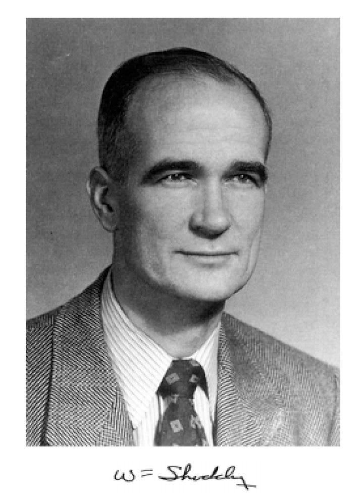
Born in London to American parents in 1910, William Bradford Shockley grew up in an 1889 Craftsman-style house at 959 Waverley Street in Palo Alto, just yards from the famed Hewlett-Packard garage. He was a precocious child, described as “ill-tempered, spoiled, almost uncontrollable, who made his doting parents’ lives miserable.” Shockley earned a bachelor’s degree at the California Institute of Technology and a PhD in theoretical physics from the Massachusetts Institute of Technology. At Bell Telephone Laboratories, he performed research in solid-state materials and served in a Naval Operations Research role during World War II.
In 1945, Shockley returned to Bell Labs to manage a group in Murray Hill, New Jersey, seeking a semiconductor replacement for the vacuum tube. Under his direction, John Bardeen and Walter H. Brattain demonstrated a germanium point-contact transistor in 1947. All three scientists received the 1956 Nobel Prize in physics “for their researches on semiconductors and their discovery of the transistor effect.”
The germanium transistor was a fragile configuration and therefore impossible to manufacture at scale easily, so Shockley went on to invent a more reliable and reproducible device, the junction transistor, in January 1948.
Who was Arnold O. Beckman?
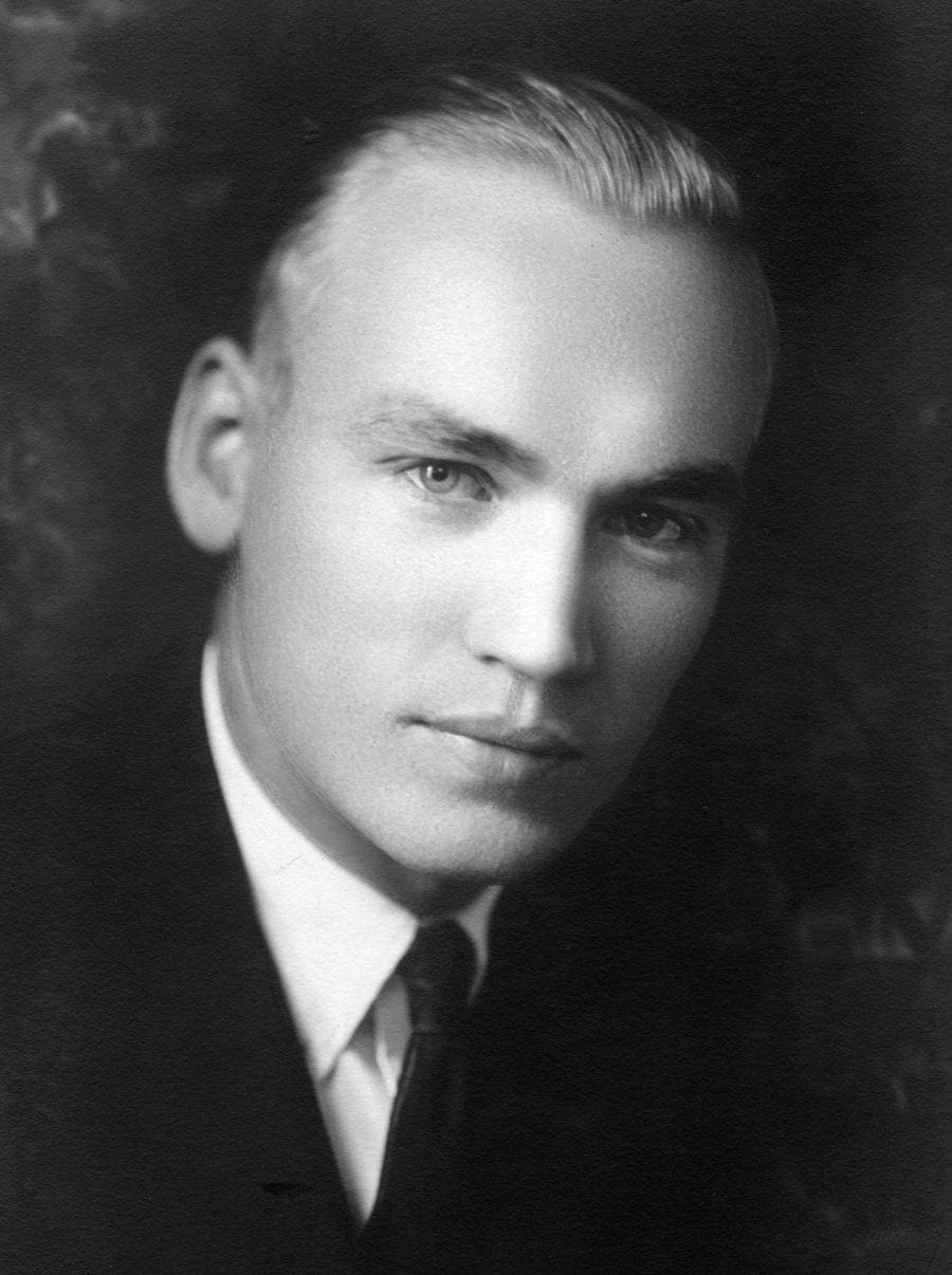
Born in Cullom, Illinois, in 1900, Arnold Orville Beckman received degrees in chemistry and chemical engineering from the University of Illinois and a doctorate in chemistry from the California Institute of Technology in 1928. While a Caltech professor, he developed an electronic pH meter to measure acidity in lemons. In 1935, he founded National Technologies Laboratories in Pasadena, California, to manufacture the device for general-purpose applications. Beckman also met Shockley, a fellow teacher, while at Caltech.
In 1940, Beckman designed a low-cost spectrophotometer, a device for measuring the intensity of light, and called it the “Model T of laboratory instruments.” In the early 1950s, he renamed his firm Beckman Instruments, Inc. In addition to being a supplier of medical, automation, and industrial equipment, Beckman Instruments developed systems to measure the components of smog in Southern California. Beckman became widely recognized for his role in encouraging the collaboration of science, technology, industry, and education to tackle the problem.
‘A glimmer of the financial possibilities’
By 1954, Shockley’s junction transistor had become the mainstay of the young semiconductor industry. New techniques, such as diffusion processing, were raising performance and predictability, and the first silicon transistors had appeared at Bell Labs and Texas Instruments (TI). Compared to germanium, silicon promised improved operation in harsh industrial and military environments but was challenging to manufacture. As Joel N. Shurkin writes in Broken Genius: The Rise and Fall of William Shockley, Creator of the Electronic Age, Shockley understood the impact transistors could have on the future, “perhaps more than almost anyone else in the world,” and “began to get a glimmer of the financial possibilities,” but he was frustrated at his stagnating career outlook. “Shockley’s over-bearing competitiveness and ham-handed approach to managing people” had generated serious issues with his peers and limited his promotion prospects, according to Lillian Hoddeson and Michael Riordan in Crystal Fire: The Birth of the Information Age.
Exploring alternative opportunities, Shockley took a leave of absence as a visiting professor at Caltech, followed by a year in Washington, D.C., as a deputy director at the Pentagon. In June 1955, he wrote to Emmy Lanning, who would become his second wife, “Think I shall try to raise some capital and start on my own.” With encouragement from his bosses at Bell, Shockley pursued financial backing from the Rockefeller family and several corporations, including TI and Raytheon, the era’s largest transistor manufacturer.
Shockley contacted Beckman, whom he knew as a fellow graduate and teacher at Caltech and with whom he had talked earlier in the year about an idea for an “electronic eye.” In September 1955, they met in the Los Angeles area and agreed “to engage promptly and vigorously in activities related to semi-conductors.” Although Beckman preferred to see the operation based near his Fullerton headquarters, 25 miles south of downtown Los Angeles, Shockley persuaded his benefactor — with the support of Frederick Terman, the provost and dean of engineering of Stanford University — to establish their venture in the Santa Clara Valley. Some believe that his mother’s home in Palo Alto was an equally important consideration.
Putting the silicon in Silicon Valley
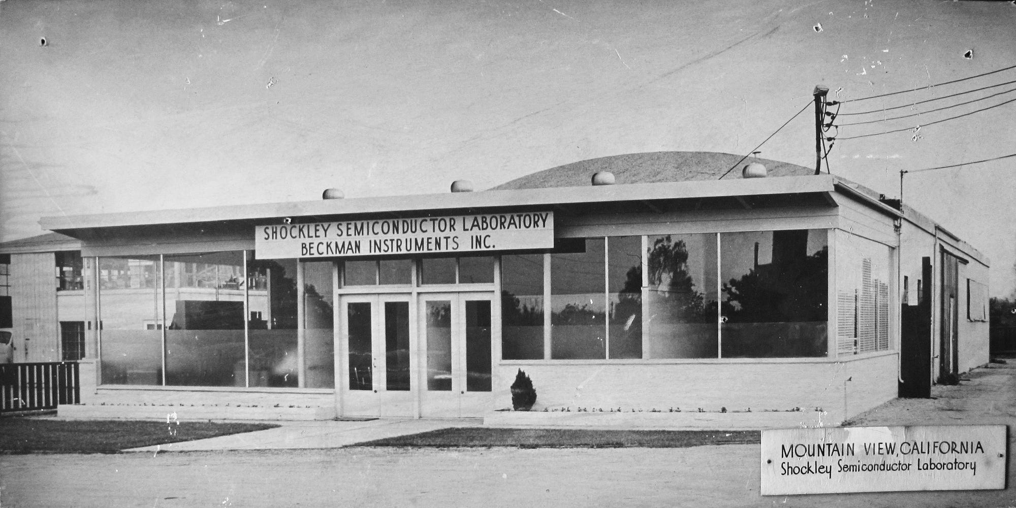
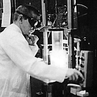
After the announcement on Valentine’s Day, 1956, Shockley spent the next six months developing his new organization. Starting from a rented Palo Alto storefront, early in 1956, he moved into a Quonset-style, former apricot packing shed at 391 San Antonio Road in Mountain View. As he told a reporter for the Los Angeles Times, Shockley set out to recruit young researchers with “hot minds” in chemistry, physics, and engineering disciplines related to semiconductors. In meeting his commitment to build “the most creative team in the world for developing and producing transistors,” this was the most fruitful aspect of Shockley’s entrepreneurial career. Early hires included Gordon Moore and Robert Noyce, Intel’s future founders; Jean Hoerni, inventor of the fundamental manufacturing process that continues to enable the semiconductor industry today; and Eugene Kleiner, a leading early venture capitalist.
The group began preparing the facility and designing specialized equipment for fabricating silicon devices. While teaching them how to grow pure crystals and diffuse P-N junctions, Shockley trained a cadre of engineers and technicians in the art and science of working with silicon. In Gordon Moore’s words, Shockley “put the silicon in Silicon Valley.” But rather than the improved silicon transistors he had promised Beckman, he focused on a complex four-layer diode, a precursor to the integrated circuit that could replace several components.
The stuff of legends
Shockley’s confrontational management style and frequent changes in direction delayed the development of revenue-generating products and triggered a confrontation with key employees. The story of their mutiny, Beckman’s failed intervention, and their exit in 1957 to found the fabulously successful Fairchild Semiconductor, based on Shockley’s original plan, is the stuff of Silicon Valley legend. Numerous books and movies have told the story, notably Crystal Fire, The Man Behind the Microchip, and the PBS video American Experience: Silicon Valley.
Shockley Semiconductor never made a profit, and Beckman sold the company at a substantial loss in 1960. Shockley became a full-time professor at Stanford, where he alienated the community with his racist theories about intelligence and eugenics. Though he was one of the most highly revered scientists of his era, he died as a public pariah in 1989. Beckman Instruments recovered from the setback and thrived in the market for sophisticated instruments and electronics. Arnold Beckman retired and became active as a philanthropist and humanitarian in science and education. He died at age 104 in 2004.
The silicon-based semiconductor industry of the Santa Clara Valley that emerged from the press conference on Saint Valentine’s Day in 1956 boomed over the following decade. The nickname Silicon Valley came into popular use in 1971. It’s interesting to contemplate how flamboyant personalities like those of Steve Jobs and Elon Musk would have shone amid the local Hollywood glitterati if not for Shockley and Beckman’s ultimate decision to set up shop in the Bay Area.
In 1998, former employees unveiled a plaque dedicated to the Shockley Semiconductor Laboratory in the sidewalk entrance. The former packing shed turned laboratory housed a succession of tenants, including a stereo store and a produce market, before being razed in 2015 to make way for a multiuse commercial development.
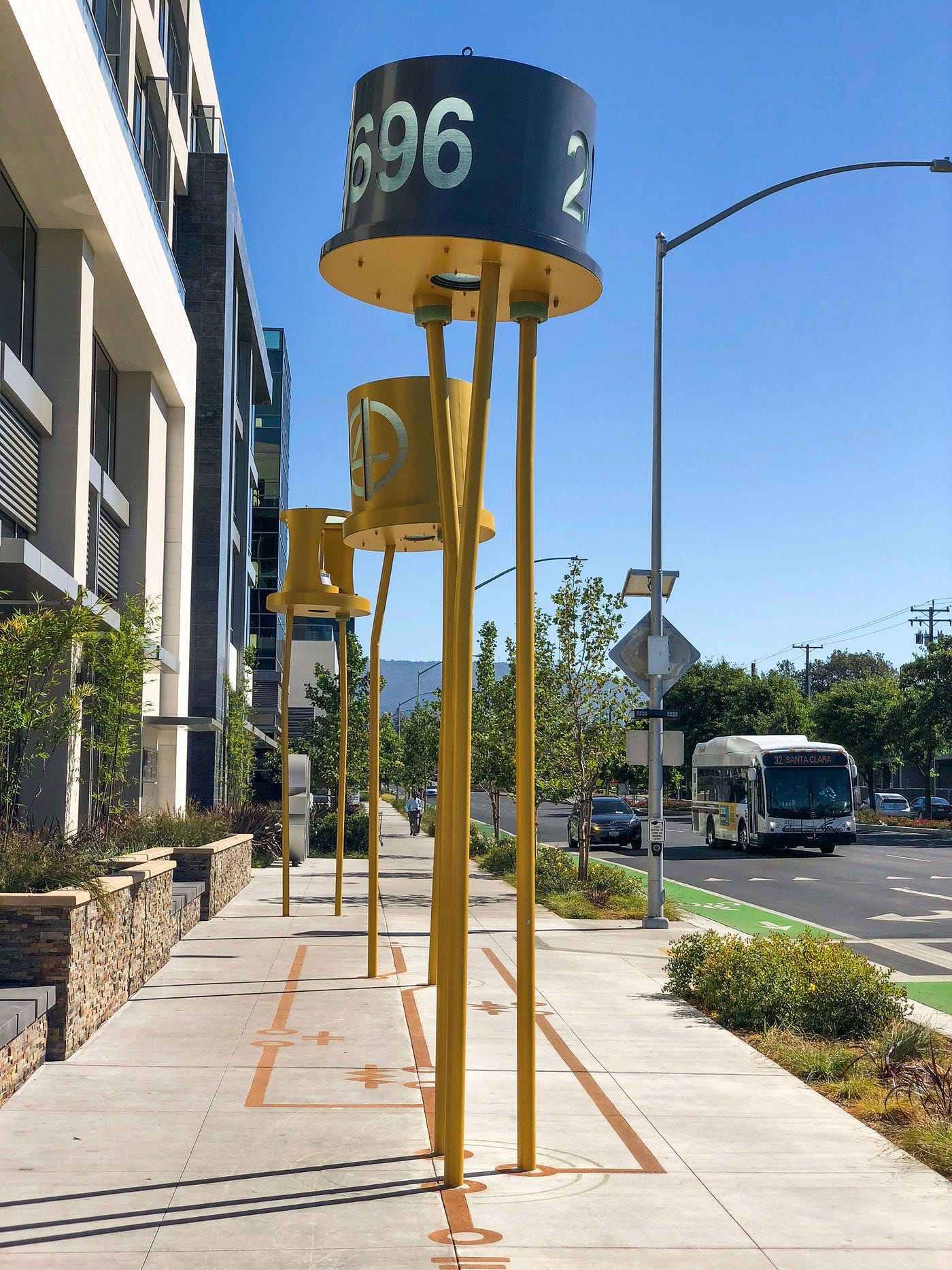
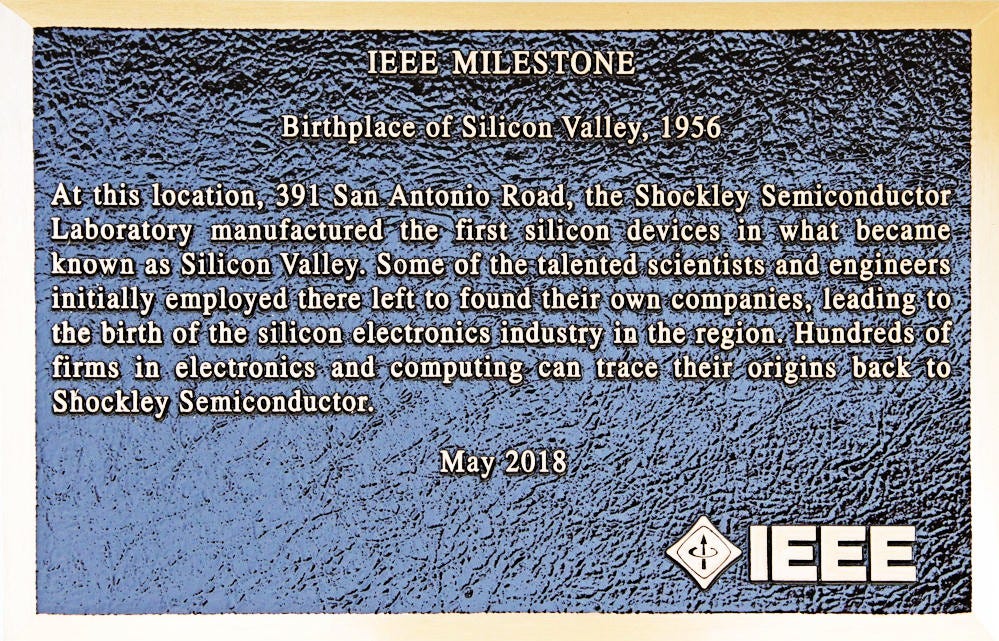
A new 391 San Antonio opened in August 2018. To commemorate its legacy, the developers incorporated three giant sculptures of semiconductor devices into the sidewalk and connected them into an oscillator circuit with “wires” painted on the sidewalk. An interpretive panel mounted on the wall includes a genealogy chart depicting the succession of companies that spun out of the lab, together with an IEEE Milestone plaque celebrating the site as the place that gave birth to silicon in Silicon Valley.
A version of this article was originally published on the @CHM blog of the Computer History Museum on February 10, 2016.
The Bold Italic is a not-for-profit media organization, and we publish first-person perspectives about San Francisco and the Bay Area. We operate under a fiscal sponsorship of a 501(c)(3).
You can become a paid subscriber. Or donate. Or learn more about us.